
Multi-Process Capability
Combine sputtering and thermal evaporation within a single platform.
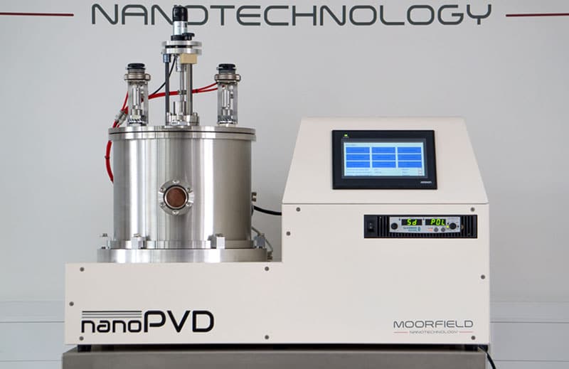
nanoPVD platform
The nanoPVD platform combines sputtering and thermal evaporation within compact, research-focused deposition systems designed for advanced materials development and thin-film process innovation.
nanoPVD enables researchers to perform advanced thin-film deposition workflows without the infrastructure complexity associated with large-scale manufacturing systems.
Designed for universities and R&D laboratories, nanoPVD systems support flexible process development, rapid experimentation and reproducible thin-film deposition.
Combine sputtering and thermal evaporation within a single platform.
Support rapid process iteration and materials experimentation.
Improve reproducibility and experimental consistency.
Expand system capability as research evolves.
Explore peer-reviewed publications and scientific references connected to Moorfield thin-film deposition systems.
| Need | Moorfield nanoPVD approach | Conventional enterprise systems |
|---|---|---|
| Research workflow focus | Designed for changing experimental objectives. | Often optimised around fixed production processes. |
| Infrastructure burden | Compact integration into research labs. | Higher facility and operational requirements. |
| Reconfiguration | Expandable configurations as research evolves. | Often slower or more complex to adapt. |
The nanoPVD platform supports sputtering, thermal evaporation and low-temperature evaporation workflows.
Yes. nanoPVD systems are designed for university and research laboratory environments.
Yes. The modular architecture supports future process expansion and capability upgrades.
Research-grade deposition without enterprise complexity.
Request configuration advice >