
Research flexibility without enterprise complexity
Industries we serve
Explore Moorfield thin-film deposition, anneal and plasma etch platforms by research area, application workflow and development environment.

Application-led platform selection
Choose your research area
Each industry page connects a research challenge to relevant Moorfield process approaches, product families and supporting application examples.

Advanced Materials Research
Flexible PVD, plasma and thermal workflows for exploratory thin films, surfaces, coatings and specialist materials research.
View industry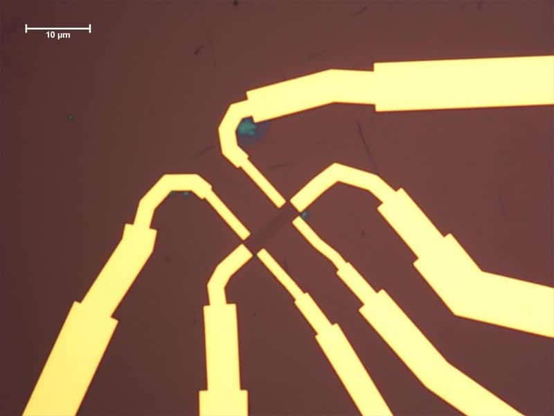
Semiconductor Prototyping
Compact process capability for rapid iteration, training, overflow and early-stage semiconductor process development.
View industry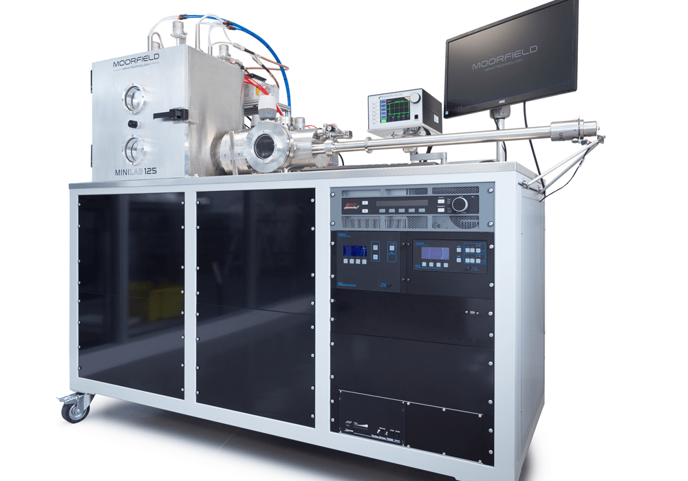
Small-batch production
MiniLab PVD options for startups and SMEs moving from R&D samples toward pilot-scale thin-film production.
View industry
Renewable Energy and PV
Deposition, anneal and glovebox-compatible workflows for photovoltaic materials, contacts and device stacks.
View industry
Optoelectronics
Flexible thin-film workflows for organic electronics, photodetectors, optical coatings, sensors and hybrid stacks.
View industry
Not sure where to start?
Use the product selector to match your application area, process constraints and laboratory environment to a suitable platform.
Use selectorBuilt for research teams, facilities and spinouts
Local process access
Bring selected deposition, plasma etch and anneal capability closer to the research group for faster iteration.
Configurable by workflow
Choose compact benchtop systems or modular platforms around materials, substrate size, gases and environmental needs.
Application evidence
Connect product selection to relevant Moorfield application notes, publications and process examples where available.
Find the right Moorfield platform for your workflow
Tell us about your material system, substrate size, process approach and laboratory constraints.