Product information / benchtop deposition, anneal and etch
Reduce the time from Lab to Fab
Build, tune, clean and pattern thin-film processes in your own lab before committing valuable cleanroom time, high-value substrates or scale-up budget.
Dedicated benchtop deposition, anneal and etch tools for advanced materials and semiconductor process development.
A focused benchtop workflow
Why customers choose a dedicated benchtop platform
Advanced materials projects rarely move in a straight line. Recipes change, substrates vary, and early experiments often involve materials or chemistries that are not yet suitable for a shared production-style tool.
Give researchers direct access to the process tools they need for daily learning, iteration and recipe development.
Keep novel materials, mixed chemistries and early-stage recipes on a dedicated platform designed for R&D flexibility.
Create repeatable process data, samples and device-relevant evidence before transferring to larger tools or external facilities.
The Moorfield nano platform is designed for that stage of development: close to the researchers, configurable to the application and repeatable enough to generate credible evidence.
Where the nano platform adds value
Map the process step to the benchtop tool
Start with the process outcome: what film needs to be made, what treatment is required, what surface or interface must be controlled and what evidence the team needs to generate.
| Process step | Customer need | Moorfield nano tool | Outcome |
|---|---|---|---|
| Deposit / grow | Create films, contacts, electrodes, dielectrics, organics or exploratory layer stacks. | nanoPVD | Research-grade films from a compact, recipe-based benchtop PVD platform. |
| Anneal / tune | Control thermal treatment after deposition or during materials development. | nanoANNEAL | Repeatable heating under controlled vacuum, inert or reactive atmospheres. |
| Clean / etch / pattern | Prepare surfaces, activate interfaces or etch delicate materials without over-processing. | nanoETCH | Dedicated low-power plasma capability for sensitive 2D and thin-film materials. |
Benchtop nano tools
Build a practical process loop at the bench
Moorfield nano systems give R&D teams the process control of a specialist vacuum tool in a benchtop format, helping labs learn faster, protect sensitive materials and build confidence before scale-up.
Build and qualify the thin-film stack
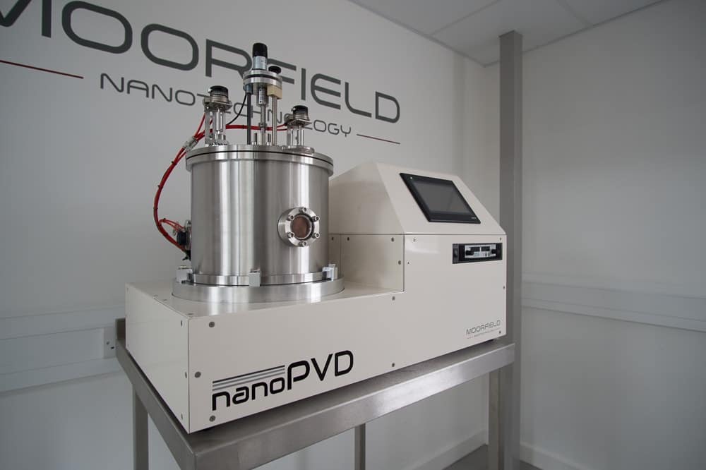
nanoPVD gives research teams a compact, configurable approach to physical vapour deposition for metals, dielectrics, transparent conducting oxides, organics and exploratory multilayer stacks.
- Develop contacts, electrodes, seed layers, barrier layers, dielectrics, TCOs, sensor coatings and optoelectronic stacks without tying up a larger production-style tool.
- Use saved recipes and touchscreen operation to improve repeatability between users and projects.
- Configure the system around the material set rather than forcing the research programme around a fixed shared tool.
Make thermal treatment part of the development loop
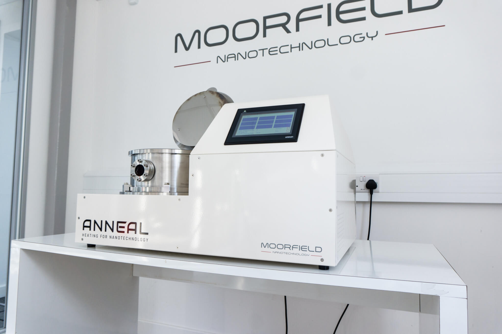
nanoANNEAL is a benchtop vacuum annealing platform for controlled thermal treatment of wafers and materials under vacuum, inert or reactive atmospheres.
- Treat samples without moving every experiment into a large shared furnace or a full PVD system.
- Control the thermal step that can influence film properties, interface quality, crystallinity and device performance.
- Develop anneal windows alongside deposition and etch work, creating a more complete benchtop process capability.

Clean, activate and etch sensitive materials
nanoETCH is a dedicated benchtop RIE platform for labs that need controlled plasma processing without relying on a shared etch tool designed for less sensitive work.
- Pattern graphene, hBN, MoS2 and other sensitive materials while exploring a useful process window instead of destroying the sample.
- Use a compact benchtop footprint to keep etch capability close to device fabrication and materials development teams.
- Save recipes, improve repeatability and reduce training burden for new users working across multiple substrates and chemistries.
Customer challenges
Why dedicated benchtop infrastructure helps
Dedicated process access can reduce friction for semiconductor R&D groups, university facilities, spinouts and advanced materials teams that need credible process evidence before scale-up.
| Challenges | Benchtop Advantages | Benefits |
|---|---|---|
| Long waits for shared equipment | Put deposition, anneal or etch capability in the research lab. | Shorter learning loops and fewer delays between experiment design and process data. |
| Unproven materials or chemistries | Use a dedicated chamber for exploratory recipes. | Protects shared tools while giving researchers freedom to explore new process windows. |
| Sensitive thin-film interfaces | Configure clean vacuum, controlled gases, gentle plasma and appropriate thermal treatment. | Improves confidence that measured performance reflects the material stack, not uncontrolled processing. |
| Multiple users and changing projects | Use touchscreen HMI, stored recipes and modular options. | Improves day-to-day usability while keeping the system flexible as the research programme evolves. |
Configuration approach
Build the right benchtop capability around the process
The right configuration starts with the process outcome, not a product list. Moorfield can help define a practical approach around deposition, anneal, plasma processing or a combined workflow.
Create or compare thin-film layer stacks
Start with nanoPVD for controlled deposition of metals, dielectrics, organics or mixed stacks in a benchtop high-vacuum platform.
Optimise film or interface properties
Use nanoANNEAL for repeatable thermal treatment under the atmosphere and temperature conditions required by the material.
Clean, activate, pattern or gently etch surfaces
Use nanoETCH for dedicated low-power plasma processing for sensitive 2D materials, thin films and exploratory recipes.
Develop a more complete process flow
Combine nanoPVD, nanoANNEAL and nanoETCH to move from deposition through thermal treatment, surface preparation and process evidence.
What to tell Moorfield
Share the process constraints that define the tool
Share the substrate size, material set, process gases, target temperatures, deposition or etch requirements, throughput expectations and any cleanroom, glovebox or safety constraints. Moorfield will recommend a nanoPVD, nanoANNEAL, nanoETCH or combined workflow configuration matched to the application.
Descriptions are indicative. Final system configuration is subject to application requirements and agreed specification.
Product FAQ
Frequently asked questions
Can Moorfield systems be specified in a university capital equipment grant application?
Yes. Moorfield can provide a formal quotation and system specification document suitable for inclusion in EPSRC, ERC, or internal university capital equipment bids. Contact the team with your process requirements and timeline.
What is the lead time for a Moorfield benchtop PVD system?
Lead times vary by configuration. Contact Moorfield after confirming your specification to receive a current delivery estimate alongside your quotation.
Can a single Moorfield system serve multiple research groups?
Yes. Moorfield systems are designed for multi-user research environments. Recipe storage, touchscreen operation, and configurable process parameters support multiple users and projects within a shared lab infrastructure.
Take control of critical semiconductor process steps at the bench
Deposit films, tune materials, prepare interfaces and etch sensitive stacks with the flexibility and repeatability needed for credible R&D.